New national identity highlights Singapore’s semiconductor capabilities, partnerships, research and manufacturing ecosystem.
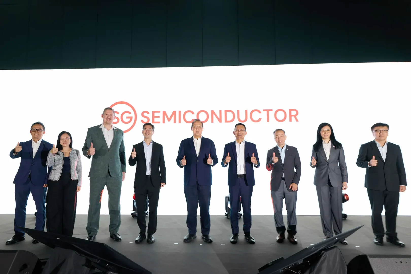
Minister for Trade and Industry (Energy and Industry) Dr Tan See Leng announced SG Semiconductor, a national identity for Singapore’s semiconductor sector, at Innovate Together 2026 on 25 September 2026. Organised by the Agency for Science, Technology and Research (A*STAR), the annual forum connects public research and industry to advance semiconductor technologies.
Jointly developed by A*STAR and the Singapore Economic Development Board (EDB), SG Semiconductor aims to raise the global visibility of Singapore’s semiconductor capabilities and provide companies and talent with a clearer way to engage the country’s ecosystem. The initiative will initially focus on public sector research and development (R&D).
Singapore’s semiconductor industry has developed over nearly six decades and spans chip design, wafer fabrication, assembly and testing, equipment and materials development and manufacturing, as well as R&D. The sector accounts for one in ten global chip output and one-fifth of global semiconductor manufacturing equipment production. From 2026 to 2030, S$800 million will be invested through the RIE Flagship in Semiconductors.
SG Semiconductor brings together capabilities in R&D, advanced manufacturing, infrastructure, industry partnerships and talent. Its work covers seven technology areas: advanced packaging, silicon photonics, power electronics, radio frequency gallium nitride, piezoelectric micro-electro-mechanical systems, flat optics and integrated circuit design.
At Innovate Together 2026, several new and expanded industry partnerships were also announced. Applied Materials and ASTAR will expand their joint laboratory through Phase 4 of their collaboration, while ASTAR and KLA will establish a process control collaboration framework. A*STAR and STATS ChipPAC will also collaborate on co-packaged optics.
In silicon photonics, ASTAR and GlobalFoundries will deepen their R&D collaboration on next-generation technologies using 300 mm wafers in Singapore. Tacta Systems and ASTAR will develop intelligent sensing technologies for robotics through A*STAR’s Lab-in-Fab platform, while Tacta Systems has opened its Singapore operations.
A new research collaboration between the National Centre for Advanced Integrated Photonics at Nanyang Technological University and Battery Age Minerals will explore germanium-based devices for data communications.
A*STAR Chief Executive Mr Beh Kian Teik said SG Semiconductor brought Singapore’s public research, universities and industry efforts under a national identity. EDB Managing Director Mr Jermaine Loy said the initiative would provide a gateway to Singapore’s ecosystem for companies developing and commercialising next-generation semiconductor technologies.
Source: Singapore Economic Development Board (EDB)